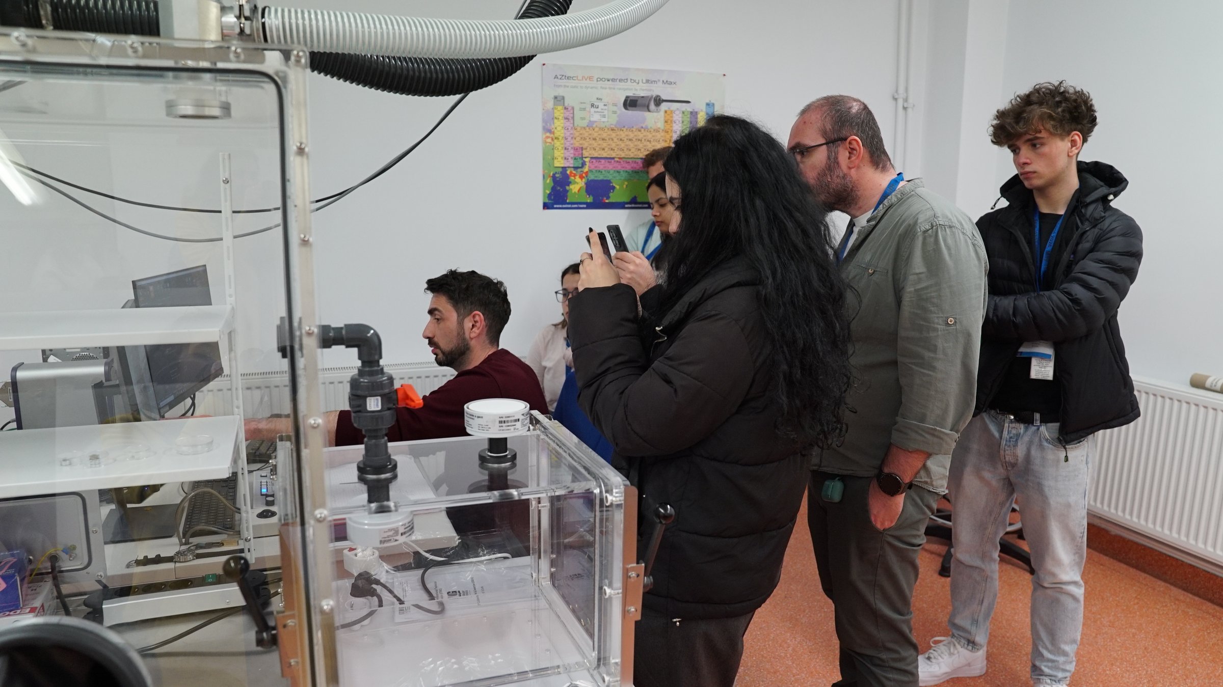
What is TIESR?
Every sample — a shard of pottery, a sliver of alloy, a fleck of tissue — carries a story written in its structure and chemistry; you just need the right instruments to read it. TIESR is where we read those stories: DFNA’s characterisation and imaging platform, gathering X-ray computed tomography, electron microscopy, mass spectrometry, atomic force microscopy, radiation spectrometry and X-ray fluorescence under one roof at IFIN-HH. (The name stands for Testing, Trials and Experiments with Radiation Sources.)
Together these instruments cover elemental, structural, morphological, and radiometric characterisation of a wide variety of samples, from archaeological objects and geological specimens to advanced materials and biological tissues. The platform supports research in archaeometry, environmental science, nuclear forensics, materials science, and the life sciences.
Instruments at a glance
Complementary analytical platforms
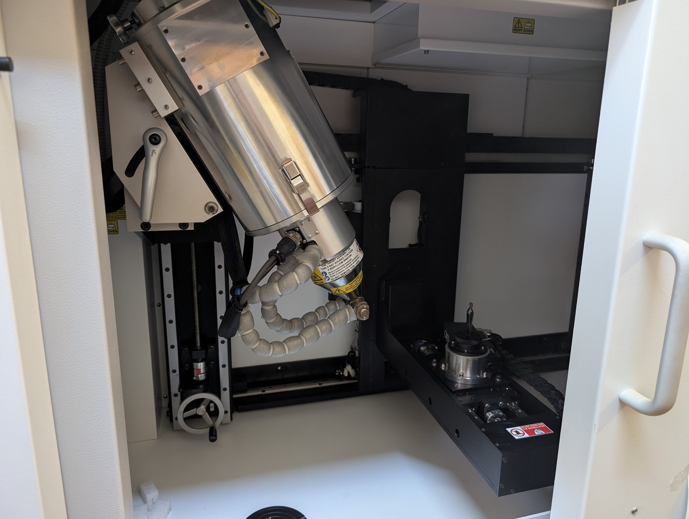
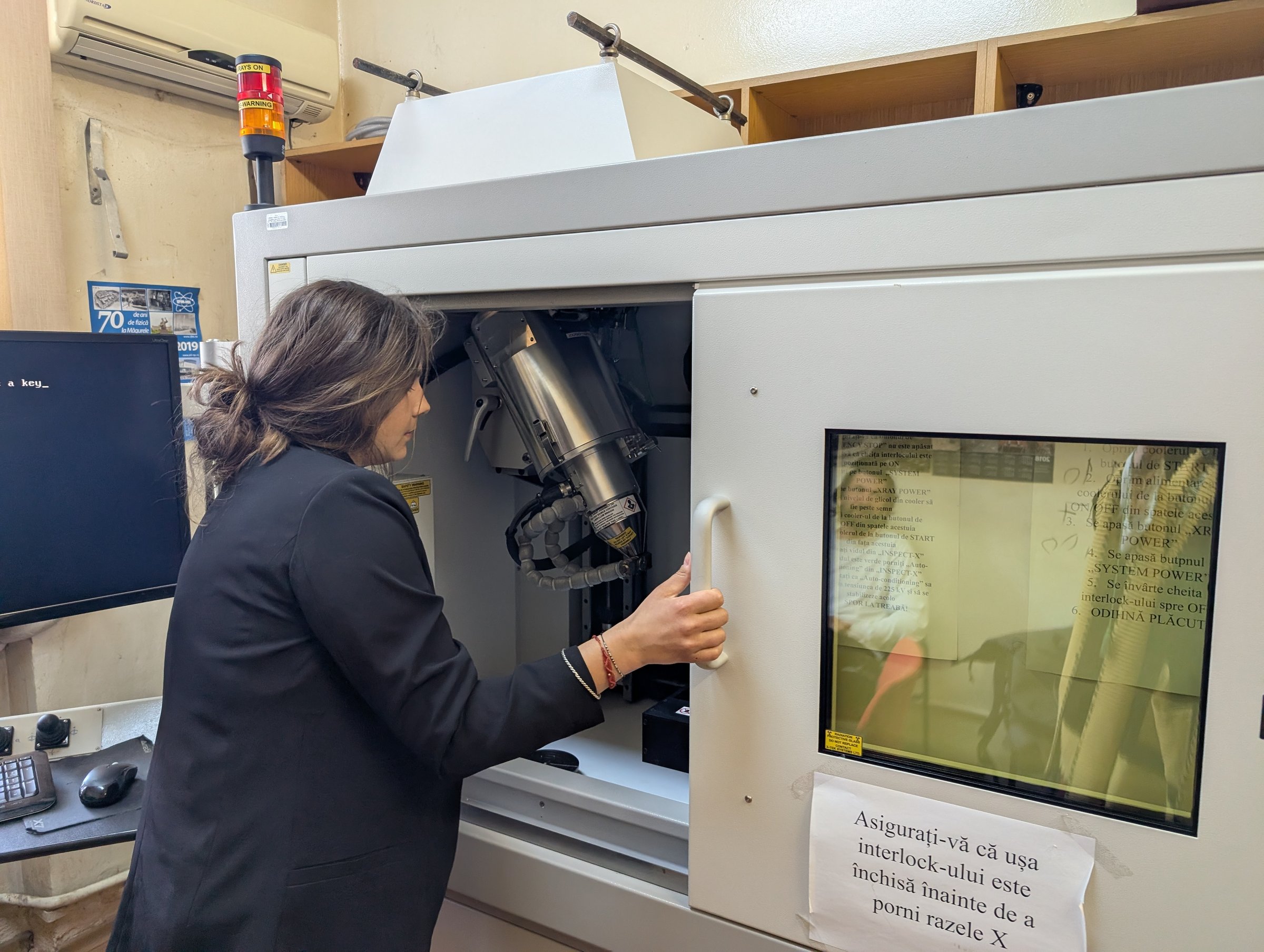
X-ray computed tomography
Nikon XTH 225 — non-destructive 3D imaging
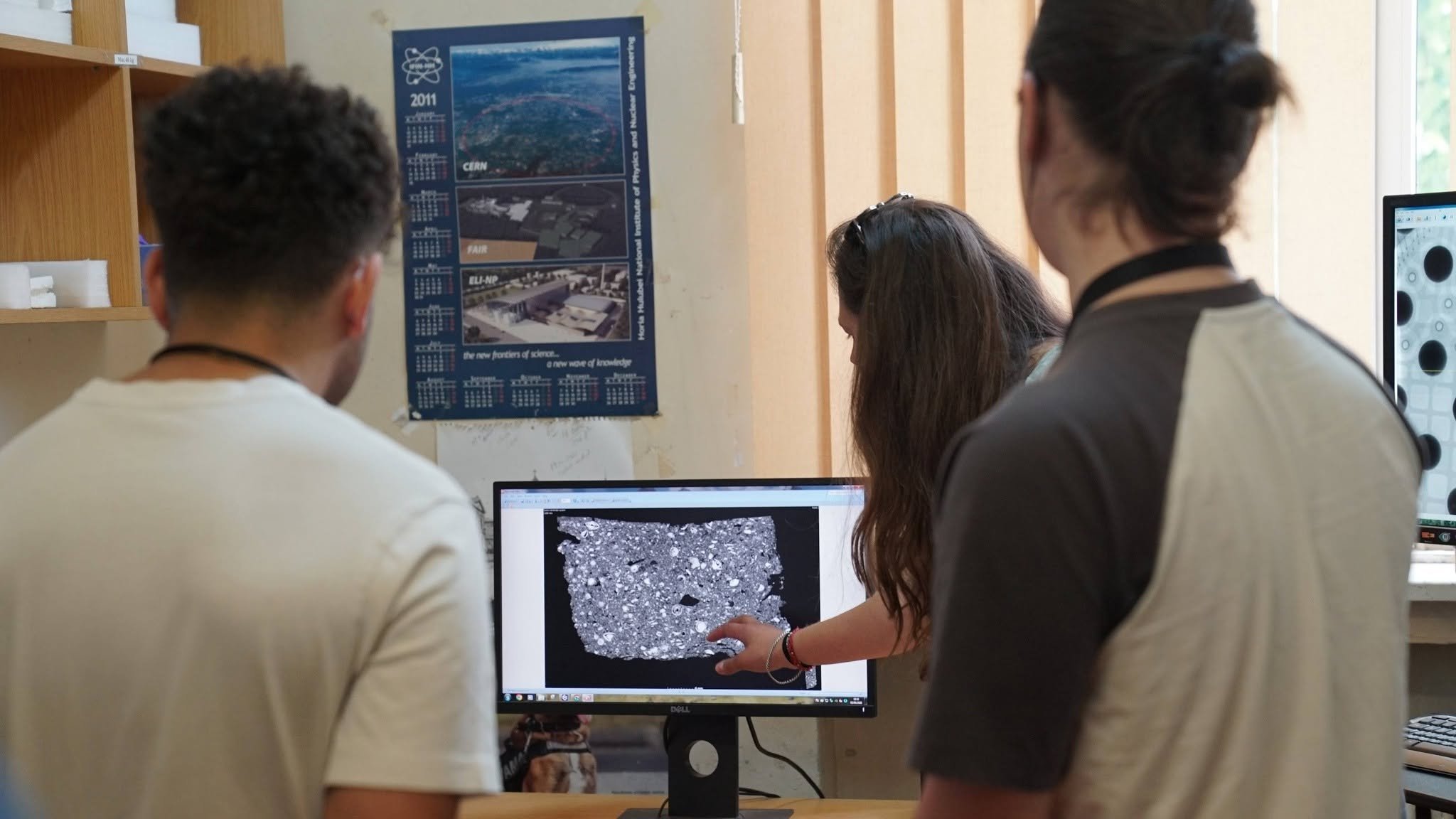
X-ray computed tomography generates a three-dimensional reconstructed image of an object by capturing a series of 2D projections as it completes a full rotation. The projections are combined by a reconstruction algorithm to produce a volumetric 3D representation that can then be virtually sectioned in three orthogonal planes — transverse, longitudinal, and frontal — to reveal interior details without cutting the sample.
The data are visualised and analysed with VGStudio MAX 3.0, enabling virtual sectioning and identification of relevant internal features.
Technical specifications
- Micro-focus X-ray source with focal spot 3 μm at 7 W, up to 225 μm at maximum power (225 W).
- Maximum object size approximately 20 cm.
- High image resolution with ultra-fast CT reconstruction.
- Suitable for ceramics, wood, metals, bones, and composite materials.
Applications
- Archaeometry — internal structure of artefacts without sampling.
- Anthropology & forensics — bone and tissue analysis.
- Nuclear forensics — inspection of suspect objects.
- Medicine & biology — non-invasive morphological study.
- Geology — analysis of rock and mineral inclusions.
Key capability
Fully non-destructive volumetric imaging of objects up to 20 cm, with virtual sectioning in three planes and sub-millimetre feature detection.
Scanning electron microscopy
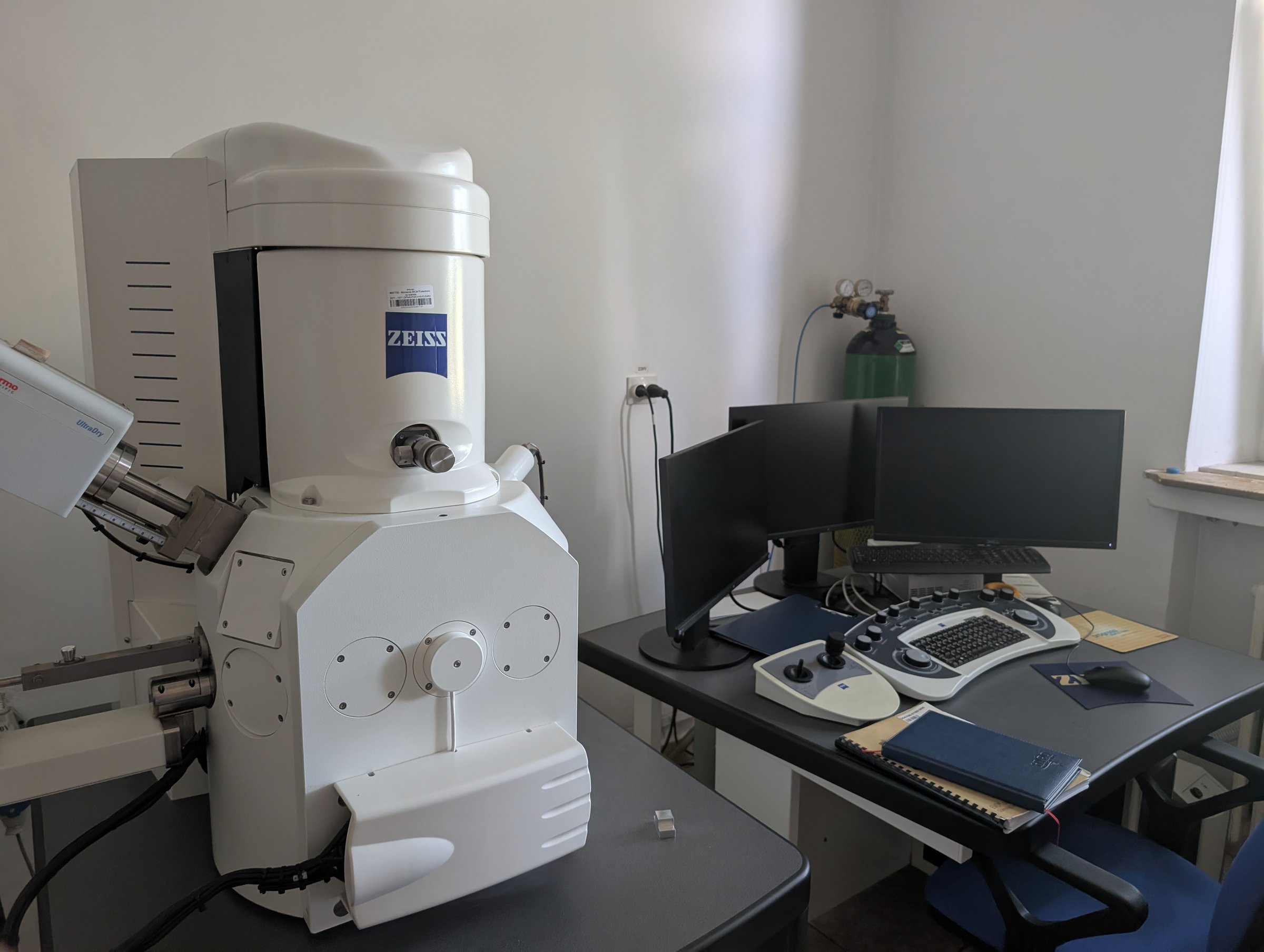
Carl Zeiss Evo MA15 with EDX — surface imaging and elemental mapping
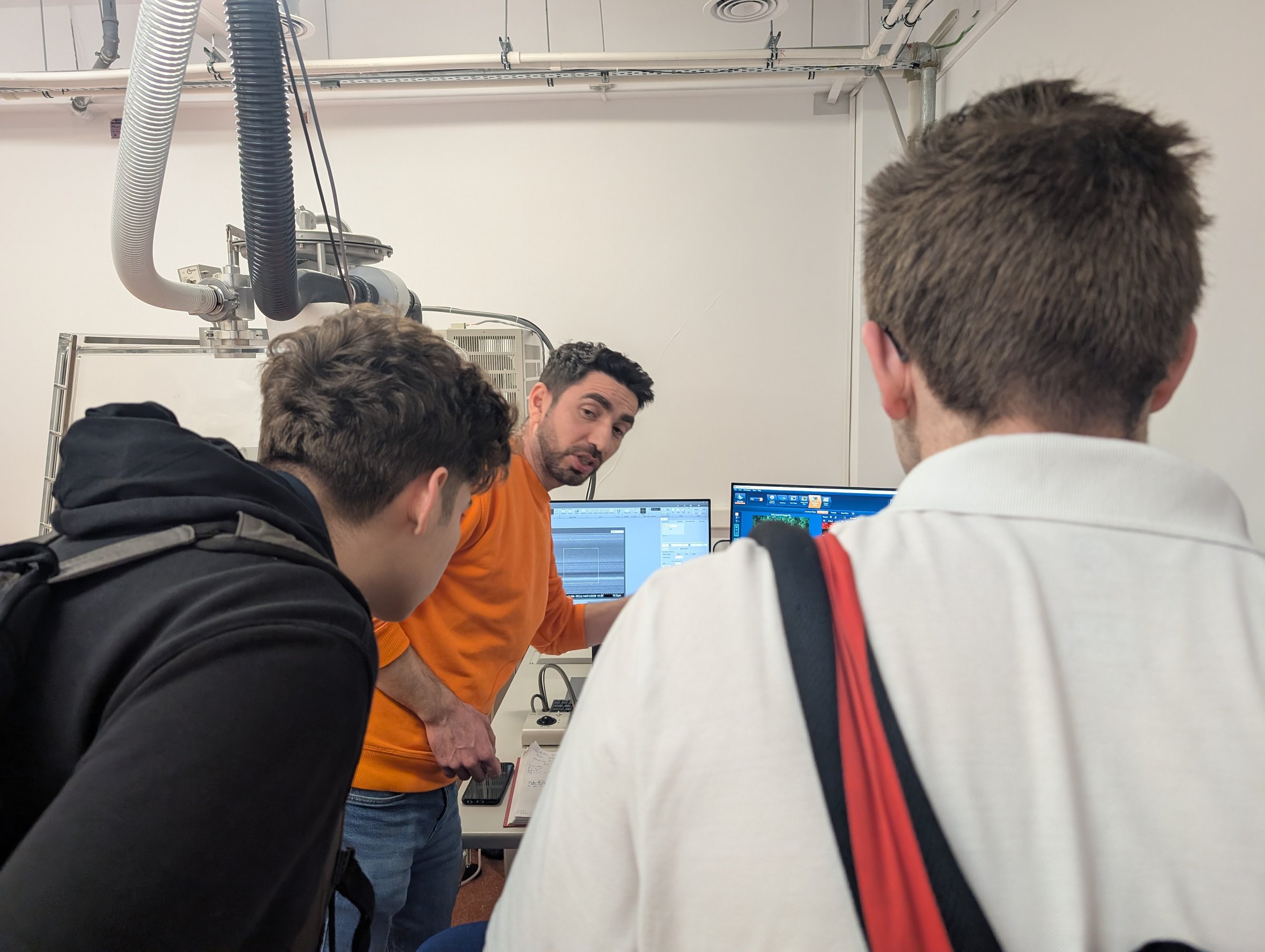
The Carl Zeiss Evo MA15 is a scanning electron microscope (SEM) that produces images with 4 nm resolution and magnifications from 50× to 1,000,000× (scale 50 nm – 20 µm). An accelerated electron beam (1–30 kV) scans the sample surface, providing detailed information on topography and morphology.
The detection system includes secondary electron detectors (standard and variable-pressure mode) and backscattered electron detectors, making it suitable for a broad range of materials: metal alloys, semiconductors, thin films, polymers, biomaterials, ceramics, geological and archaeological specimens.
Energy Dispersive X-ray Spectroscopy (EDX)
The instrument is equipped with an EDX system that detects X-rays produced by the electron beam–sample interaction. It can identify elements from beryllium (Be) to plutonium (Pu) with an energy resolution of 129 eV. Results are delivered as X-ray spectra, point analyses on selected image regions, or full 2D elemental maps.
Key capabilities
- 4 nm resolution, ×50 to ×1,000,000 magnification.
- EDX: Be–Pu elemental identification, 129 eV resolution.
- Point analysis and 2D elemental mapping.
- Variable pressure mode for uncoated or hydrated samples.
Laser ablation ICP-MS
NexION 300X — trace elemental composition at ppb precision
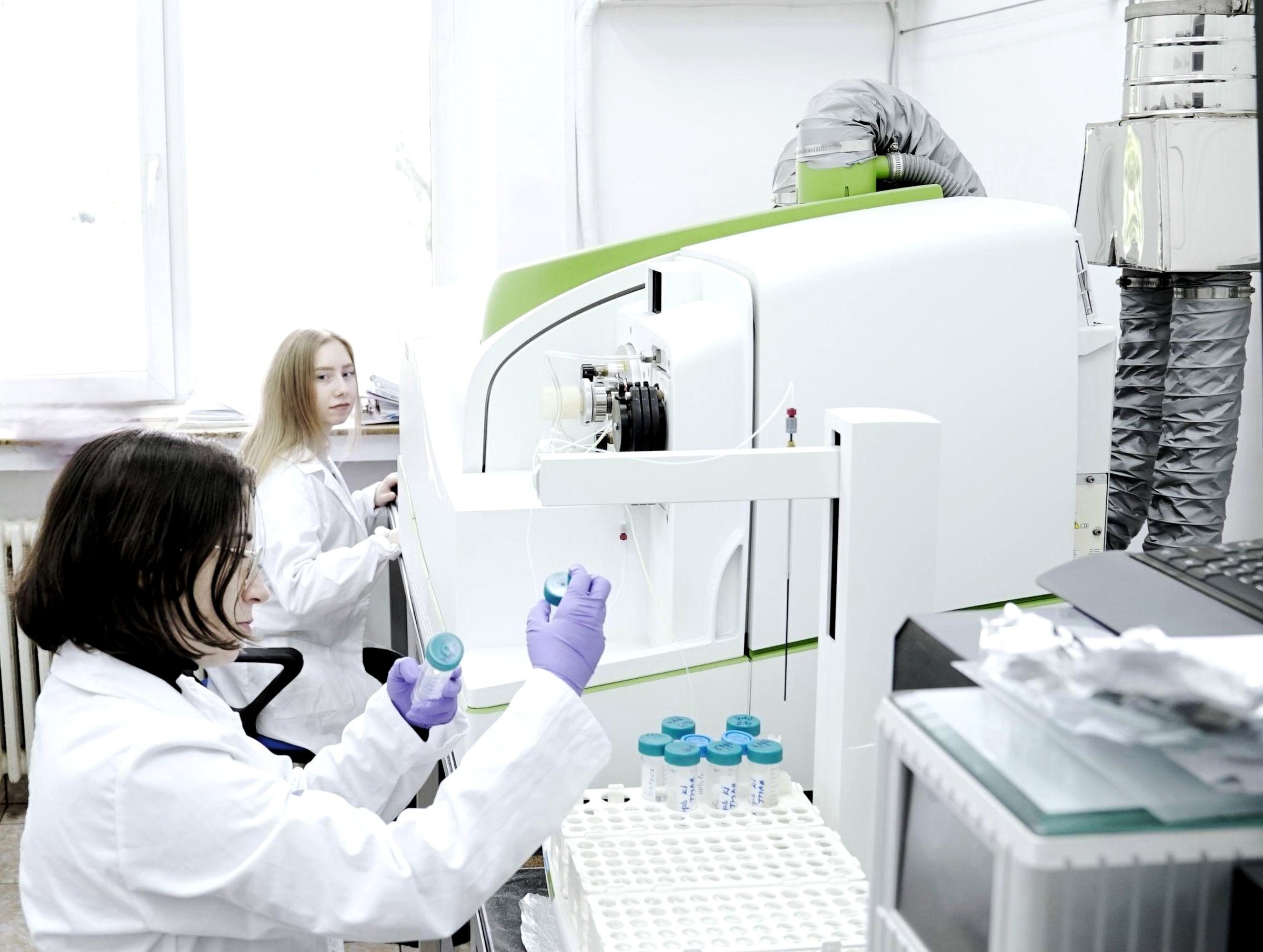
The PerkinElmer NexION 300X Inductively Coupled Plasma Mass Spectrometer (ICP-MS) at DFNA provides elemental composition analysis from sodium (Na) to uranium (U) for a wide variety of sample types — chemical solutions, archaeological objects, geological specimens, and more. Results can reach ppb (parts per billion) precision, making it one of the most sensitive elemental analysis tools available.
Laser ablation mode (LA-ICP-MS)
A UV laser vaporises a tiny volume of material from the sample surface. The ablated material is transported by helium to the ICP-MS where it is ionised and measured. The impact on the sample is quasi-non-destructive: the ablation spot is invisible to the naked eye. This mode analyses the surface composition to a depth of a few micrometres and is ideal for solid, heterogeneous, or precious samples.
Solution mode
Dissolved samples are introduced as solutions, providing a more global, whole-sample elemental analysis. This mode requires sample dissolution and dilution, but delivers the highest accuracy for homogeneous matrices.
Key capabilities
- Elements Na to U, ppb sensitivity in solution mode.
- Solid samples via UV laser ablation — quasi-non-destructive.
- Applicable to geological, archaeological, chemical, and environmental samples.
Atomic force microscopy — NANOMAT
Nanoscale imaging and mechanical characterisation of micro- and nanostructured materials
The instrument
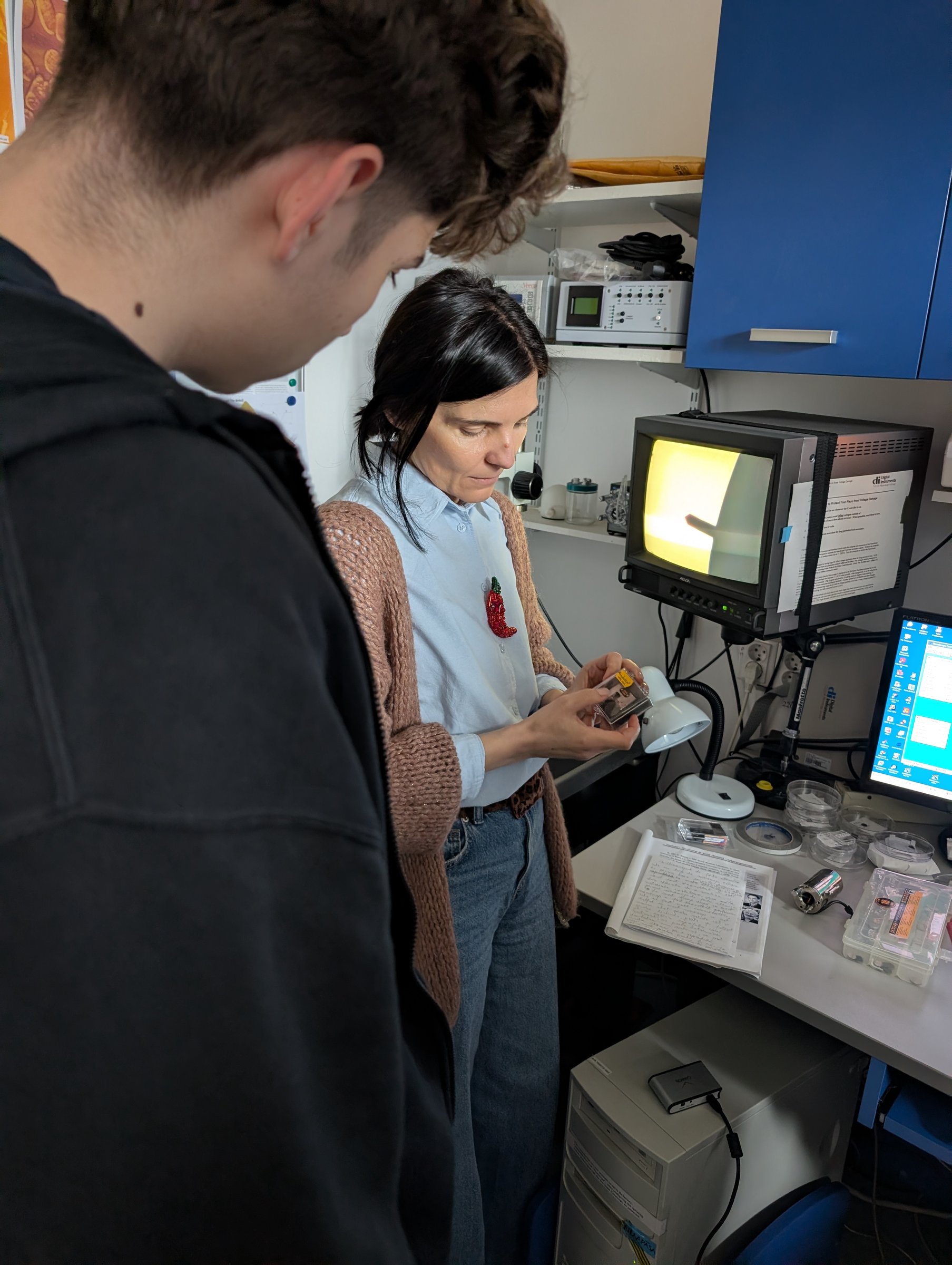
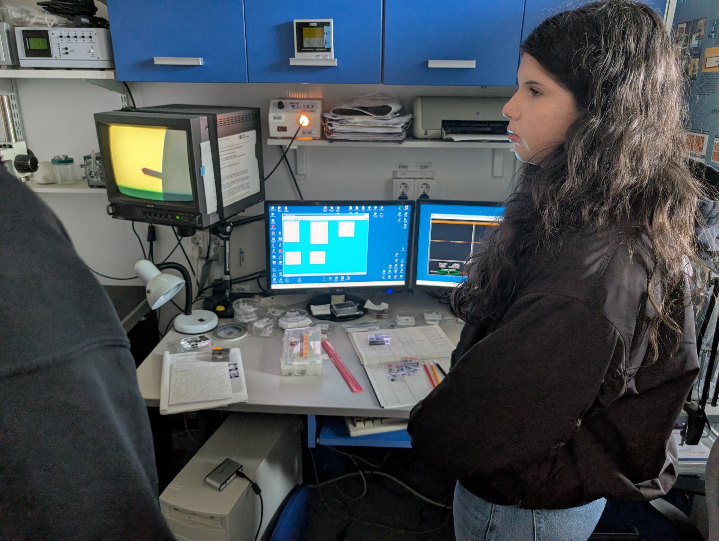
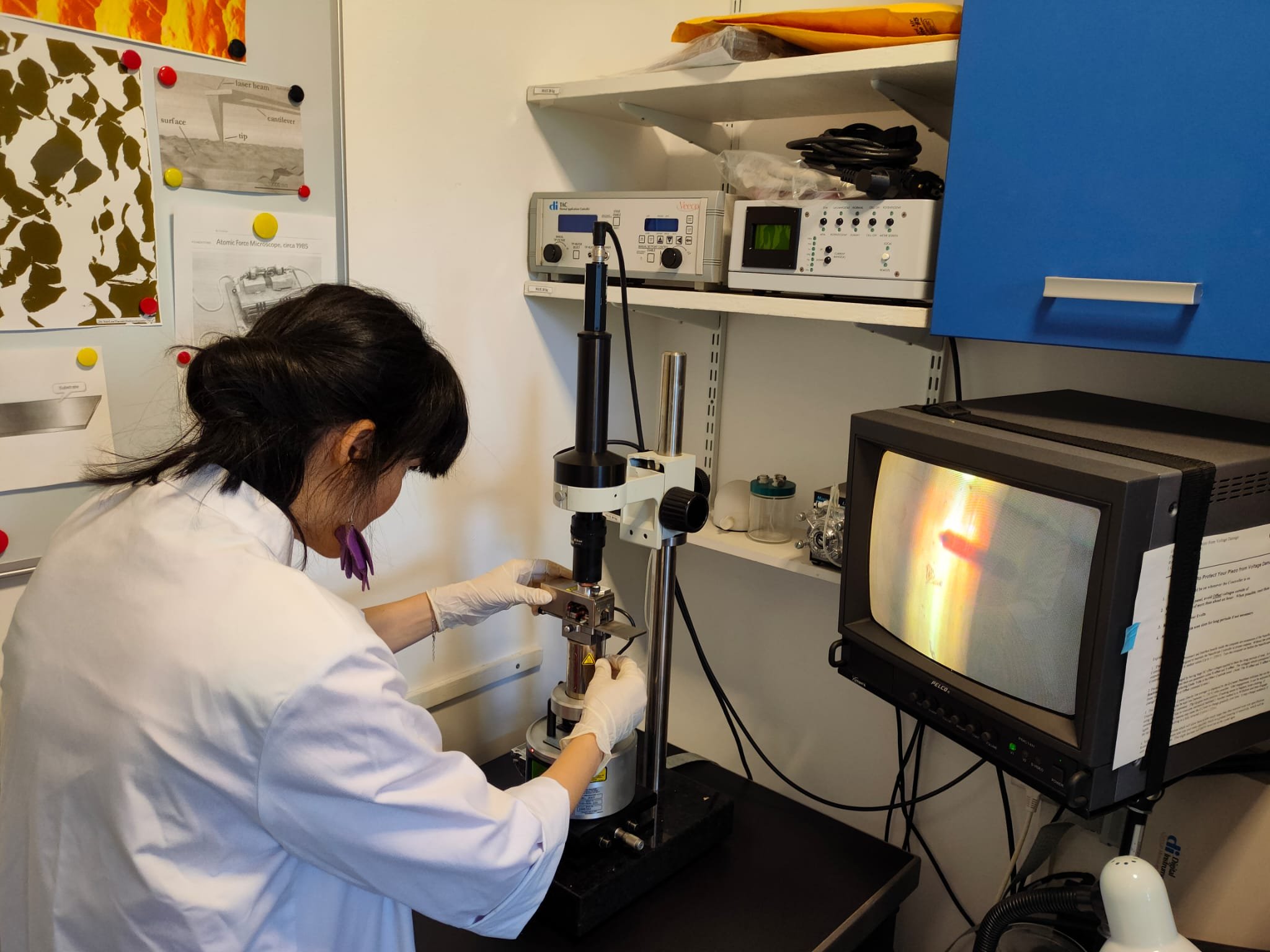
Atomic Force Microscopy (AFM) maps surfaces with a sharp tip at the end of an oscillating cantilever, resolving features down to 1–5 nm in all three dimensions. Within DFNA, the AFM is the heart of the NANOMAT laboratory for micro- and nanostructured materials: a MultiMode NanoScope III A (Digital Instruments / Veeco), operated mainly in tapping mode — gentle enough for soft, fragile or loosely adsorbed samples.
- Imaging in air and liquid; samples need no metal or carbon coating.
- Mechanical properties via nanoindentation (local hardness) and nanoscratching (wear, adhesion) — at scales conventional indenters cannot reach.
- Heater–cooler stage from −35 °C to +250 °C for biological samples and polymers.
- Housed in a clean positive-pressure enclosure for long, contamination-free acquisitions.
From single molecules to wide surveys
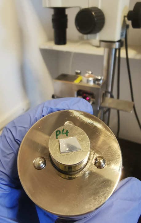
Three interchangeable scanner heads let the same instrument zoom from ultra-high-resolution detail to wide-area surveys — scan ranges of 7 × 7 μm² XY (5.5 μm Z), 15 × 15 μm² XY (3.6 μm Z) and 190 × 190 μm² XY (5.7 μm Z). Samples up to 15 mm in diameter are mounted on stainless-steel magnetic discs and placed directly on the scanner.
Sample preparation
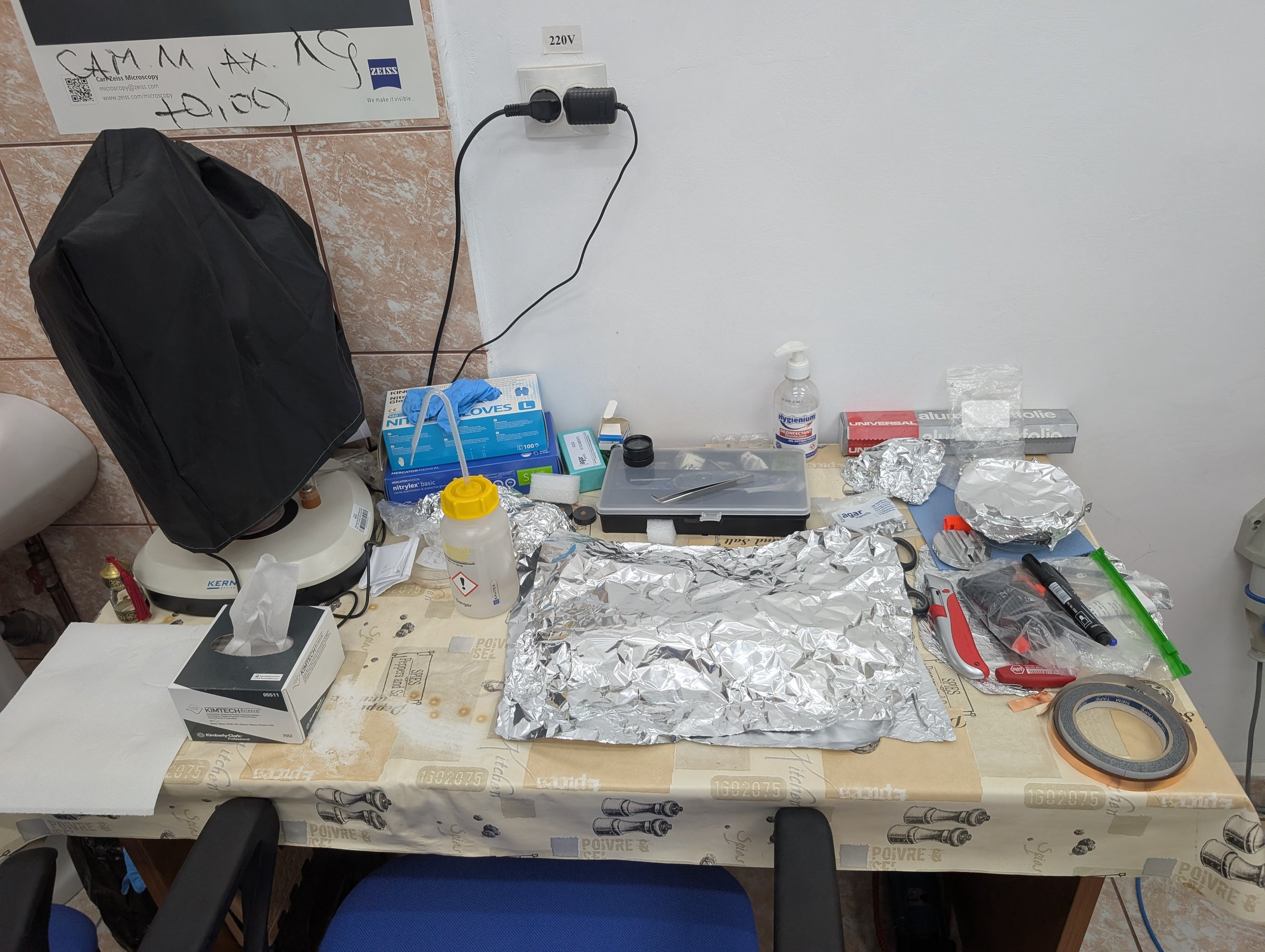
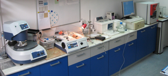
Reliable nanoscale imaging starts with a well-prepared surface. NANOMAT runs its own preparation suite — a Buehler precision saw for sectioning metals, ceramics, biomaterials and minerals, a grinder–polisher that takes surfaces to a mirror finish, an ultrasonic bath for final cleaning, plus oven, thermostat bath and analytical balance for drying, conditioning and weighing.
Radiation spectrometry
β, γ, and α detection with NaI(Tl) and CsI(Tl) scintillators
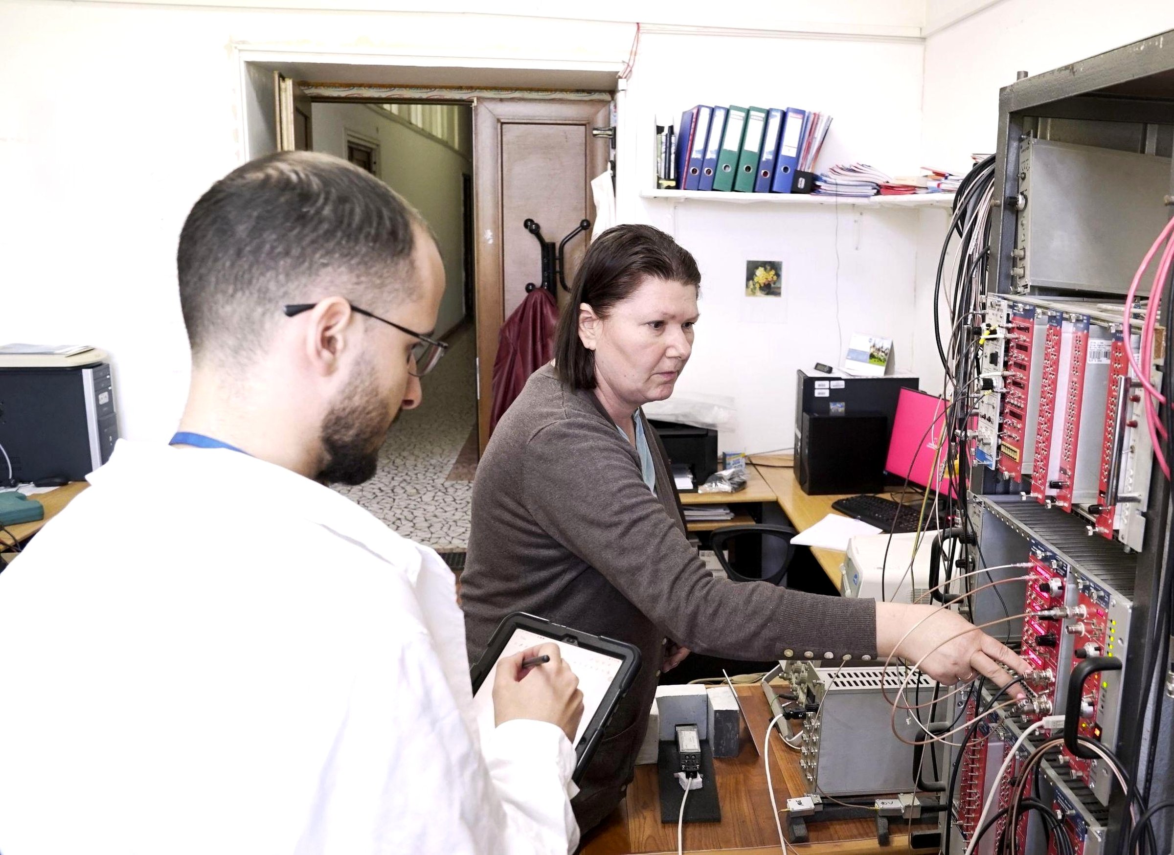
TIESR operates a dedicated installation for beta, gamma, and alpha spectrometry using inorganic scintillator detectors based on NaI(Tl) and CsI(Tl) crystals. This setup is used to characterise and evaluate detection systems, including the measurement of detection efficiency and energy resolution for different scintillator geometries and materials.
The platform supports research on novel detector materials for radiation monitoring, nuclear forensics, and environmental measurement. Measurements can be configured for a range of source geometries and source-detector distances to suit specific experimental requirements.
Main applications
- Evaluation of detection efficiency and energy resolution for scintillator crystals.
- Development and testing of new radiation detection materials.
- Environmental radioactivity measurements.
- Nuclear forensics and safeguards-related studies.
X-ray fluorescence spectrometry
Portable and fixed XRF for rapid, non-destructive elemental analysis
Portable EDXRF — Bruker Tracer 5i
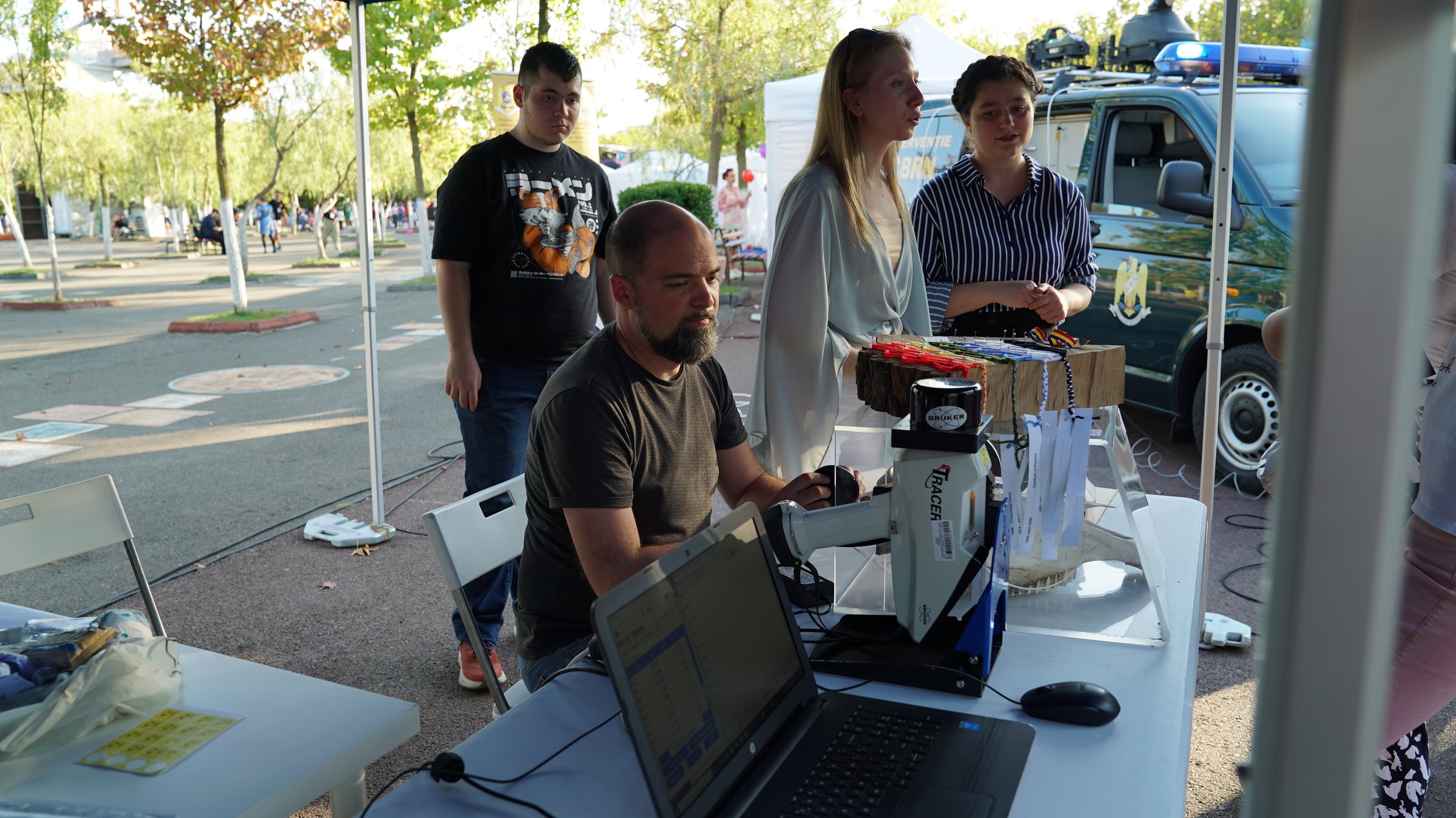
The Bruker Tracer 5i uses Energy Dispersive X-ray Fluorescence (EDXRF) to determine elemental composition from magnesium (Mg) to uranium (U) in virtually any solid or powder sample — in the laboratory or in situ (museums, archaeological sites, collections). Its portability and fast analysis make it ideal for cultural heritage studies and field campaigns.
- X-ray tube: Rh anode, voltage up to 40 kV.
- Beam collimation: 8 mm or 3 mm focal spot (software-selectable).
- Silicon Drift Detector (SDD): 40 mm² area, resolution 120 eV ± 5 eV.
- Optional He purge for improved light-element detection (down to Na, Z = 11).
- Detection limits: few ppm for medium-Z elements; ~50 ppm for high-Z (Pb, Au, actinides).
- Penetration depth: up to ~1 mm, providing bulk-representative results.
Fixed XRF — SPECTRO MIDEX M
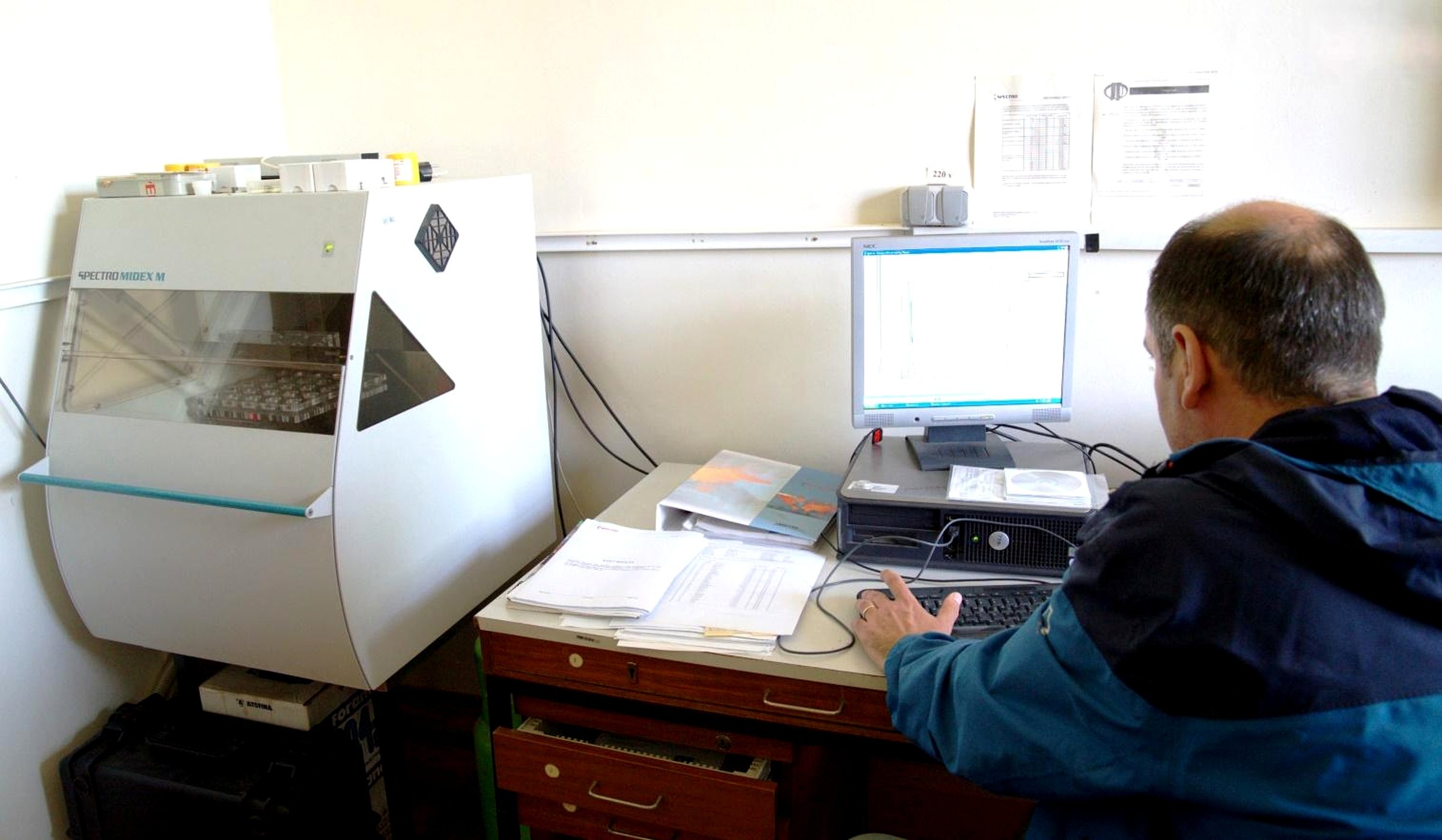
The SPECTRO MIDEX M is a stationary multifunctional X-ray spectrometer designed for rapid, point-focused, non-destructive analysis of precious metals in jewellery and a wide variety of alloys and materials. It covers elements from sodium (Na) to uranium (U).
- Mo anode X-ray tube, maximum voltage 50 kV.
- Si Drift Detector (SDD), Peltier-cooled; 8 μm Be window.
- Energy resolution: <170 eV for the Mn Kα line.
- Sample chamber: 540 × 600 × 250 mm; motorised stage with 260 × 250 × 150 mm travel at 2.5 μm resolution.
- Collimators: 0.1, 0.3, 0.5, 1, and 2 mm (software-selectable).
- Dual video system for sample visualisation on monitor.
- Calibration models: empirical and fundamental parameters (FPM), including Compton scatter method for trace elements.
Applications
Multi-technique approach for demanding scientific questions
Archaeometry
Non-destructive imaging and elemental characterisation of artefacts, pigments, metals, ceramics, bones, and textiles using CT, SEM-EDX, XRF, and ICP-MS.
Geology & environment
Mineral and rock analysis, environmental radioactivity monitoring, and trace-element mapping in geological samples.
Materials science
Surface characterisation, thin film analysis, semiconductor inspection, and nanometre-scale topography with AFM and SEM.
Nuclear forensics
Non-destructive identification and characterisation of radioactive and non-radioactive materials for safeguards and forensic applications.
Detector development
Evaluation of detection efficiency and energy resolution for new scintillator materials; testing of radiation sensing concepts.
Life-science imaging
AFM and electron microscopy of cells, tissues and biomolecules — resolving structure and surfaces down to the nanometre.
Cultural heritage
In-situ portable XRF on museum collections and on-site at archaeological excavations without sampling.
Nano-bio interfaces
AFM imaging and mechanical characterisation of biological samples — bacteria, proteins, DNA, dental tissues — at nanometre resolution.
Research it powers
How the TIESR platform connects to DFNA's research directions
Access, services, and visits
Analytical services for professionals and outreach for education
Analytical services and collaborations
Researchers and professionals from universities, research institutes, cultural heritage institutions, hospitals, and industry are welcome to contact us to discuss access to TIESR instruments. The platform is well suited for multi-technique characterisation campaigns where complementary methods are needed — for example combining CT, SEM-EDX, AFM, ICP-MS, and XRF on the same set of samples.
Together with our team, we can help you identify the most appropriate combination of techniques, design a feasible measurement plan, and estimate experimental time and costs. For enquiries and collaboration proposals, please use the contact details on the Contact page.
Visits for schools and universities
We regularly host guided visits for schools and universities who wish to learn how imaging and spectrometry techniques are applied in science and cultural heritage. Visits include an introduction to the principles behind each instrument and examples of real scientific projects carried out at TIESR.
Visits can be organised throughout the year by prior arrangement. For the Romanian "Școala altfel" programme, places can be limited, so we strongly recommend that teachers and coordinators apply well in advance via the Contact page.
Gallery
Instruments and activities at TIESR