

Coincidence Doppler Broadening Spectroscopy (CDBS) and Positron Annihilation Lifetime Spectroscopy (PALS)
Responsabili: Florin Constantin, Marin Focșăneanu, Marta Petruneac
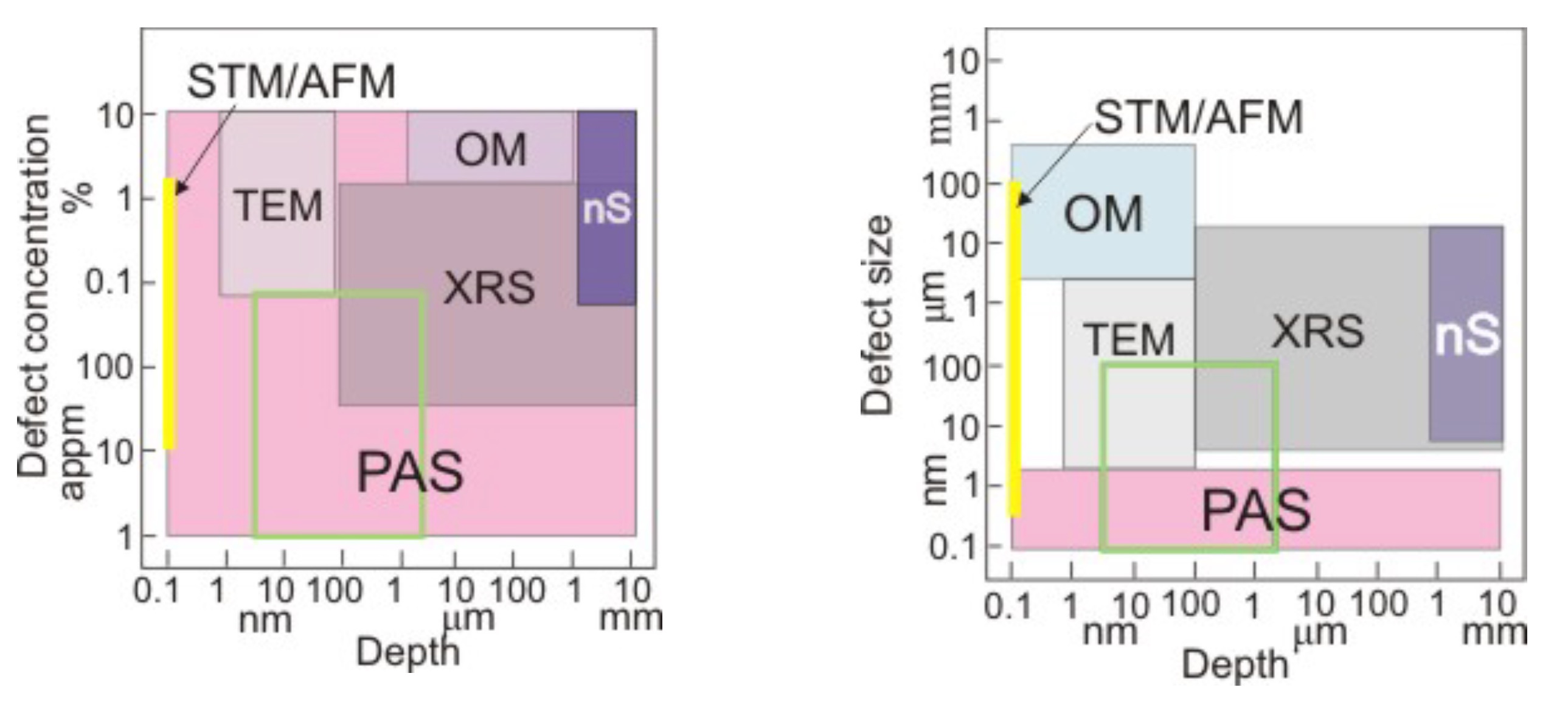
Positron Annihilation Spectroscopy (PAS) is an established analytical technique used to investigate the internal structure of materials,
and likewise a nondestructive method and sensitive at the molecular (sub-nanometer) level. Developing high quality positron spectroscopy
experiments can aid in the understanding of materials evolution over time in damaging environments, or precisely monitor material behaviour during fabrication and processing.
In order to analyze and study the materials of interest we are able to simultaneously apply two different measuring techniques of positron annihilation spectroscopy, i.e.:
• Positron Annihilation Lifetime Spectroscopy (PALS) which provides information on the electronic density of the annihilation site, because the positron lifetime is sensitive to the size,
but also to the concentration of defects in the material. Following the latest methodological developments, the PALS acquisition system is now a digital one, which has obvious advantages,
such as online data acquisition, offline use of filters, while maintaining the temporal resolution of the analog system, but with a considerably shorter acquisition time.
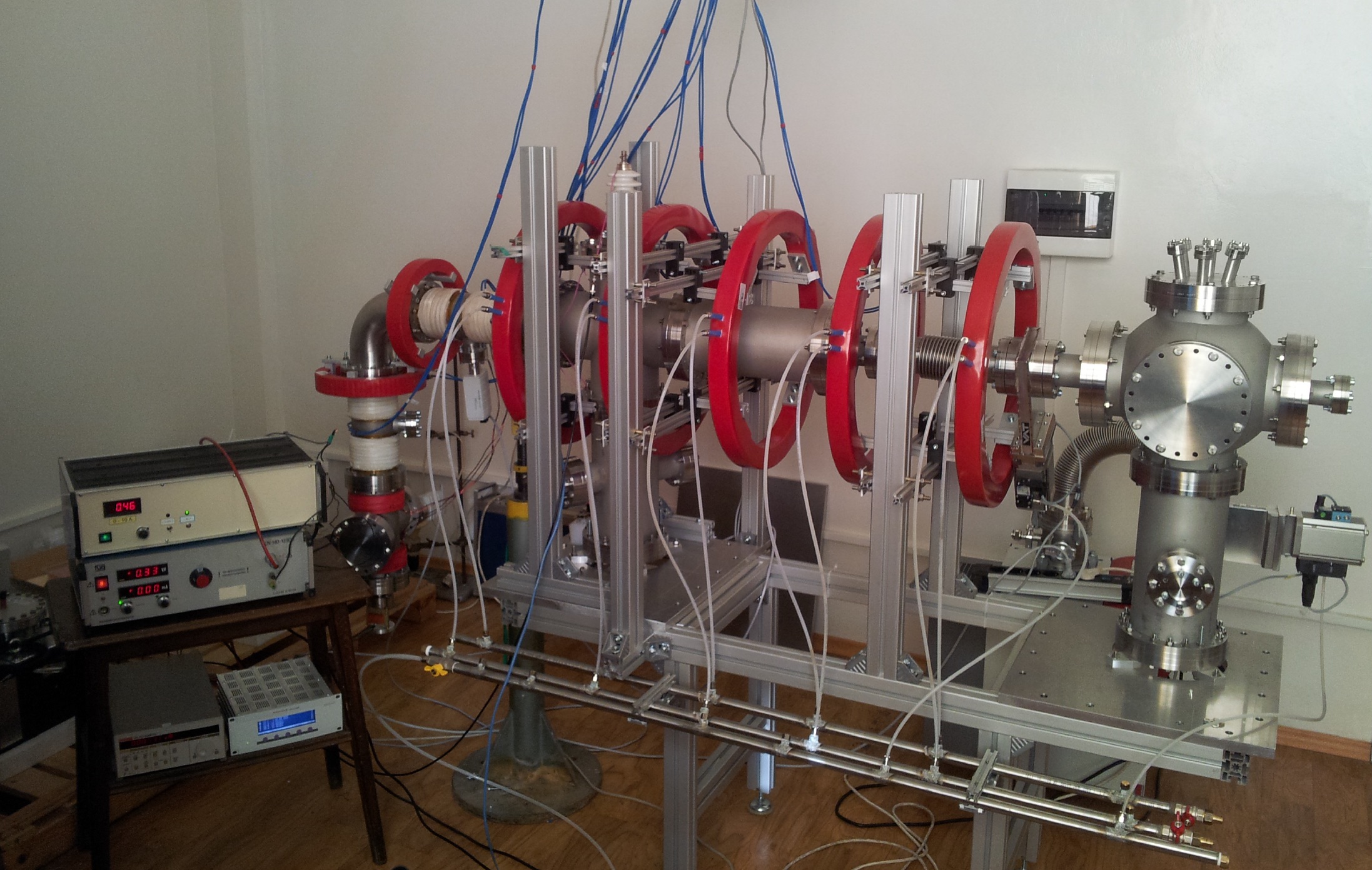
As an example (photo on the left), this system was used in the study of a polyethylene membrane superficially implanted with copper ions aiming to understand the influence of the copper ions on the sample’s properties.
• Coincidence Doppler Broadening Spectroscopy (CDBS), a technique that concerns obtaining the impulse distribution of electrons from the studied medium providing
information about the chemical vicinity surrounding the annihilation site.
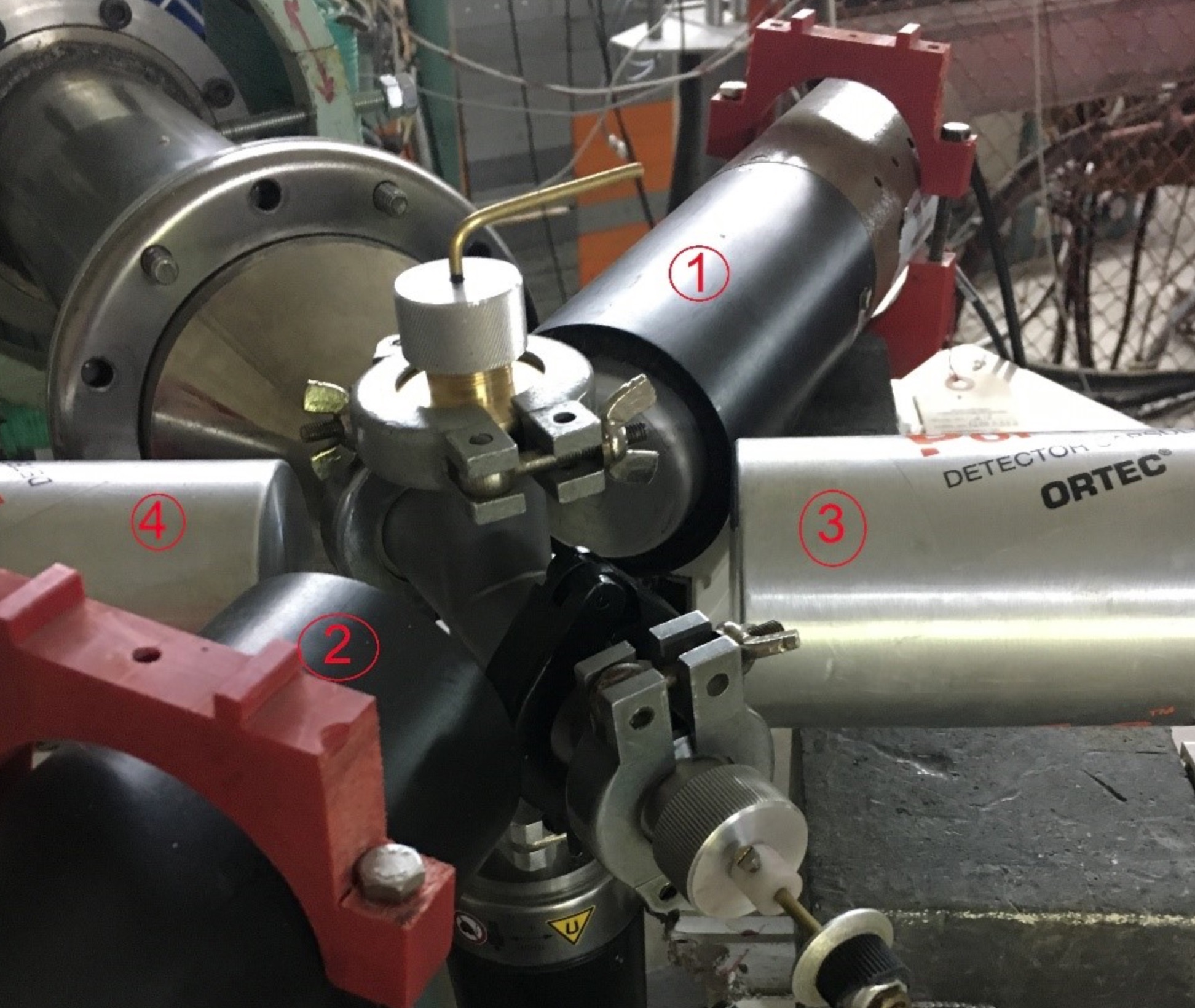
Both ion implantation and positron annihilation spectroscopy measurements were performed using the device shown in Figure 1 in order to ensure that the vacuum is not interrupted and therefore the sample is not contaminated.
The device contains in the center a rotating aluminum support with the role of dissipating heat during implantation. The sample is placed on this support which can be rotated 360 degrees as a means to allow the sample
exposure to the ion beam and subsequently to the positron source. The positron source, in the form of a small metal disk, is placed at the end of a rod with the role of pressing the source on the implanted face of the sample,
in the center of the PAS arrangement.
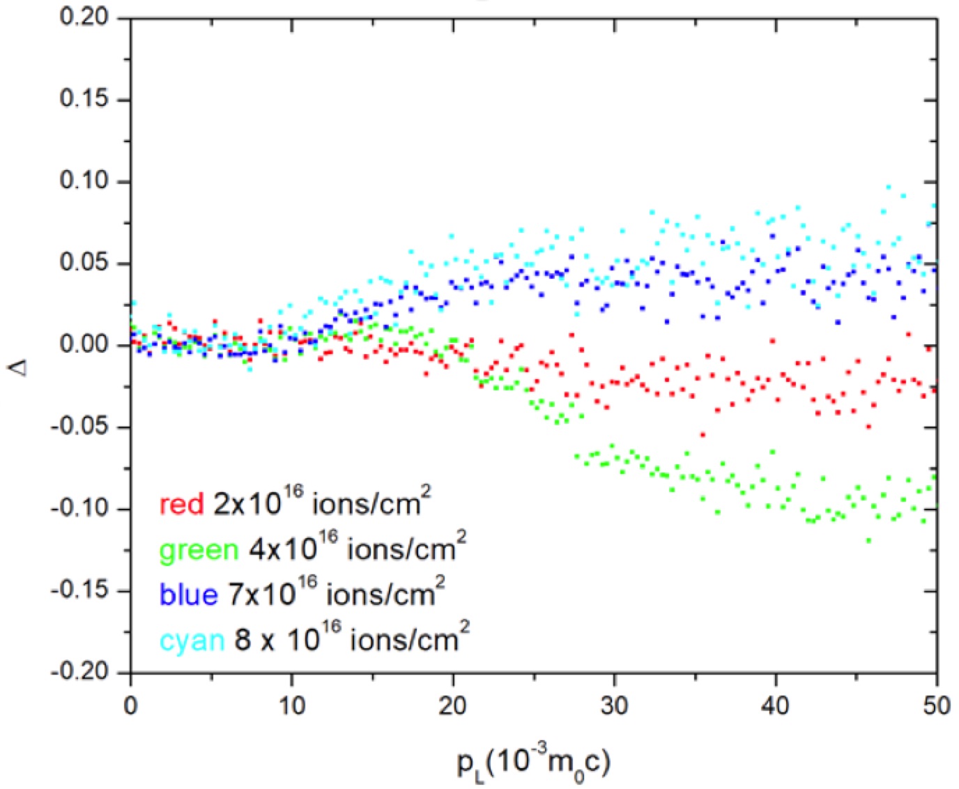
Positron annihilation spectroscopy data examples obtained on a Nafion membrane implanted with copper ions are shown in the Figure 2 and Figure 3.
For further details you are welcome to take into consideration the references presented below and likewise to contact us for more detailed information.
References:
[1] F. Constantin, M. Focsaneanu, M. Petruneac, Romanian Journal of Physics 65, 901 (2020)
[2] F. Constantin et al., Digest Journal of Nanomaterials and Biostructures Vol. 6, No 2, April - June 2011, p. 543 - 548

